- 您现在的位置:买卖IC网 > Sheet目录1905 > ATMEGA324PA-MCHR (Atmel)MCU AVR 32KB FLASH 20 MHZ 44QFN
2011 Microchip Technology Inc.
Preliminary
DS41458B-page 323
PIC16(L)F1526/27
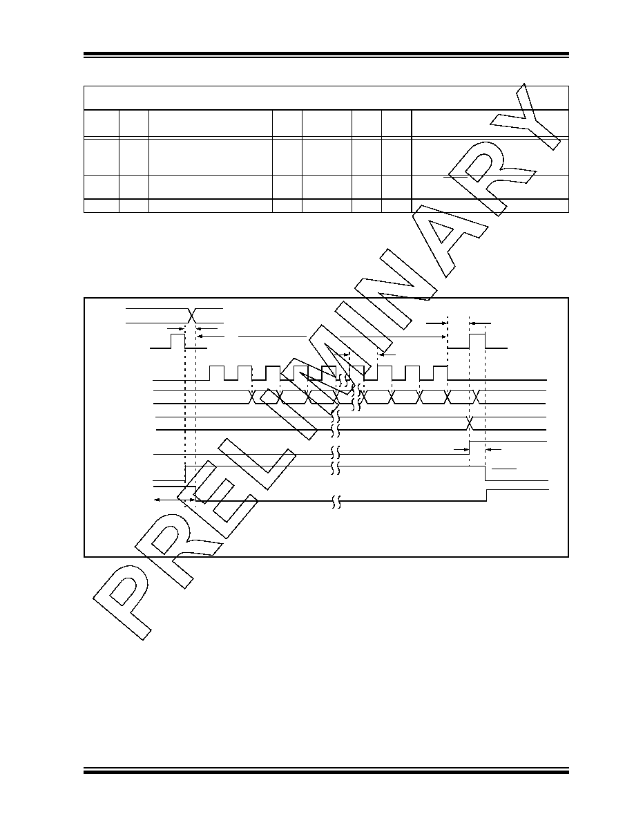
TABLE 25-8:
PIC16(L)F1526/27 A/D CONVERSION REQUIREMENTS
FIGURE 25-11:
PIC16(L)F1526/27 A/D CONVERSION TIMING (NORMAL MODE)
Standard Operating Conditions (unless otherwise stated)
Operating temperature
-40°C
TA +125°C
Param
No.
Sym.
Characteristic
Min.
Typ
Max.
Units
Conditions
AD130* TAD
A/D Clock Period
1.0
—
9.0
sTOSC-based
A/D Internal RC Oscillator
Period
1.0
1.6
6.0
s
ADCS<1:0> = 11 (ADRC mode)
AD131
TCNV
Conversion Time (not including
Acquisition Time)(1)
—11
—
TAD
Set GO/DONE bit to conversion
complete
AD132* TACQ
Acquisition Time
—
5.0
—
s
*
These parameters are characterized but not tested.
Data in “Typ” column is at 3.0V, 25°C unless otherwise stated. These parameters are for design guidance only and are not
tested.
Note 1:
The ADRES register may be read on the following TCY cycle.
AD131
AD130
BSF ADCON0, GO
Q4
A/D CLK
A/D Data
ADRES
ADIF
GO
Sample
OLD_DATA
Sampling Stopped
DONE
NEW_DATA
76
5
3
2
1
0
Note 1:
If the A/D clock source is selected as RC, a time of TCY is added before the A/D clock starts. This allows the
SLEEP
instruction to be executed.
1 TCY
4
AD134
(TOSC/2(1))
1 TCY
AD132
发布紧急采购,3分钟左右您将得到回复。
相关PDF资料
ATMEGA3250PV-10AUR
MCU AVR 32K FLASH 10MHZ 100TQFP
ATMEGA3250V-8AI
IC AVR MCU 32K 8MHZ 100TQFP
ATMEGA328P-15AZ
MCU AVR 32K FLASH 15MHZ 32-TQFP
ATMEGA32L-8PJ
IC MCU AVR 32K 5V 8MHZ 40-DIP
ATMEGA32M1-AUR
IC MPU AVR 32K 20MHZ 32TQFP
ATMEGA48PA-MMNR
MCU AVR 4KB FLASH 20MHZ 28QFN
ATMEGA644P-B15MZ
IC MCU 8BIT 64KB FLASH 32VQFN
ATMEGA644V-10PU
IC AVR MCU FLASH 64K 40DIP
相关代理商/技术参数
ATMEGA324PA-MN
功能描述:8位微控制器 -MCU AVR 32KB FLSH 1KB EE 2KB SRAM-20MHz 105C RoHS:否 制造商:Silicon Labs 核心:8051 处理器系列:C8051F39x 数据总线宽度:8 bit 最大时钟频率:50 MHz 程序存储器大小:16 KB 数据 RAM 大小:1 KB 片上 ADC:Yes 工作电源电压:1.8 V to 3.6 V 工作温度范围:- 40 C to + 105 C 封装 / 箱体:QFN-20 安装风格:SMD/SMT
ATMEGA324PA-MNR
功能描述:20 MHZ, QFP, 105C 制造商:microchip technology 系列:AVR? ATmega 包装:剪切带(CT) 零件状态:在售 核心处理器:AVR 核心尺寸:8-位 速度:20MHz 连接性:I2C,SPI,UART/USART 外设:欠压检测/复位,POR,PWM,WDT I/O 数:32 程序存储容量:32KB(16K x 16) 程序存储器类型:闪存 EEPROM 容量:1K x 8 RAM 容量:2K x 8 电压 - 电源(Vcc/Vdd):1.8 V ~ 5.5 V 数据转换器:A/D 8x10b 振荡器类型:内部 工作温度:-40°C ~ 105°C(TA) 封装/外壳:44-VFQFN 裸露焊盘 供应商器件封装:44-VQFN(7x7) 标准包装:1
ATMEGA324PA-MU
功能描述:8位微控制器 -MCU AVR 32KB 1KB EE 20MHz 2KB SRAM 5V RoHS:否 制造商:Silicon Labs 核心:8051 处理器系列:C8051F39x 数据总线宽度:8 bit 最大时钟频率:50 MHz 程序存储器大小:16 KB 数据 RAM 大小:1 KB 片上 ADC:Yes 工作电源电压:1.8 V to 3.6 V 工作温度范围:- 40 C to + 105 C 封装 / 箱体:QFN-20 安装风格:SMD/SMT
ATMEGA324PA-MUR
功能描述:8位微控制器 -MCU AVR 32KB FLSH 1KB EE 2KB SRAM-20MHz IND RoHS:否 制造商:Silicon Labs 核心:8051 处理器系列:C8051F39x 数据总线宽度:8 bit 最大时钟频率:50 MHz 程序存储器大小:16 KB 数据 RAM 大小:1 KB 片上 ADC:Yes 工作电源电压:1.8 V to 3.6 V 工作温度范围:- 40 C to + 105 C 封装 / 箱体:QFN-20 安装风格:SMD/SMT
ATMEGA324PA-PN
功能描述:8位微控制器 -MCU AVR 32KB FLSH 1KB EE 2KB SRAM-20MHz 105C RoHS:否 制造商:Silicon Labs 核心:8051 处理器系列:C8051F39x 数据总线宽度:8 bit 最大时钟频率:50 MHz 程序存储器大小:16 KB 数据 RAM 大小:1 KB 片上 ADC:Yes 工作电源电压:1.8 V to 3.6 V 工作温度范围:- 40 C to + 105 C 封装 / 箱体:QFN-20 安装风格:SMD/SMT
ATMEGA324PA-PU
功能描述:8位微控制器 -MCU AVR 32KB 1KB EE 20MHz 2KB SRAM 5V RoHS:否 制造商:Silicon Labs 核心:8051 处理器系列:C8051F39x 数据总线宽度:8 bit 最大时钟频率:50 MHz 程序存储器大小:16 KB 数据 RAM 大小:1 KB 片上 ADC:Yes 工作电源电压:1.8 V to 3.6 V 工作温度范围:- 40 C to + 105 C 封装 / 箱体:QFN-20 安装风格:SMD/SMT
ATMEGA324PA-W
功能描述:8位微控制器 -MCU AVR 32KB 1KB EE 20MHz 2KB SRAM 5V
RoHS:否 制造商:Silicon Labs 核心:8051 处理器系列:C8051F39x 数据总线宽度:8 bit 最大时钟频率:50 MHz 程序存储器大小:16 KB 数据 RAM 大小:1 KB 片上 ADC:Yes 工作电源电压:1.8 V to 3.6 V 工作温度范围:- 40 C to + 105 C 封装 / 箱体:QFN-20 安装风格:SMD/SMT
ATMEGA324P-B15AZ
功能描述:8位微控制器 -MCU 32KB FLASH AUTO 125Deg revision B RoHS:否 制造商:Silicon Labs 核心:8051 处理器系列:C8051F39x 数据总线宽度:8 bit 最大时钟频率:50 MHz 程序存储器大小:16 KB 数据 RAM 大小:1 KB 片上 ADC:Yes 工作电源电压:1.8 V to 3.6 V 工作温度范围:- 40 C to + 105 C 封装 / 箱体:QFN-20 安装风格:SMD/SMT